
The semiconductor industry in India is one of the fasts growing Industry. Semiconductors are tiny chips used in phones, cars, computers, defence systems, and many other modern devices. Therefore, their demand is increasing every year. At the same time, India is investing heavily in chip design and manufacturing. Students interested in building a career in electronics, VLSI, and semiconductor engineering can explore our engineering and competitive exam courses to strengthen their academic foundation and career preparation.
What is Semiconductor Engineering?
Semiconductor engineering is the study of making and improving tiny electronic chips. These chips are called semiconductors. They are used inside mobile phones, laptops, cars, televisions, medical machines and many other devices.
The semiconductors help electronic devices work properly. They control the flow of electricity inside a device. Because of this, a phone can turn on, a computer can process data, and a car can use smart features.
Therefore, semiconductor engineers design, test and develop these chips. They work to make devices faster, smaller, smarter and more energy-efficient. As technology grows, semiconductor engineering is becoming an important field for the future.
Why are semiconductors important for India?
The semiconductor industry in India is important because it supports almost every modern industry. These tiny chips are used in mobile phones, cars, defence systems, medical devices, telecom networks and many other machines. Their importance can be viewed in multiple dimensions
Economically, the semiconductor industry in India can bring big opportunities for growth, investment and jobs. According to official reports, India’s Semiconductor market is expected to reach USD 100 billion by 2030. This opens up more factories, investment, and skilled jobs.
Internationally, semiconductors are very much in demand all across the world. Through the semiconductor industry in India, the country can become a trusted partner in the global chip supply chain in the semiconductor sector. This can also push India’s position in Technology Diplomacy.
At the domestic level, semiconductors are important for India’s everyday needs. They are required in smartphones, electric vehicles, railway systems, defence equipment, among others. Therefore, local chip design and manufacturing can push India towards ‘Atmanirbhar’.
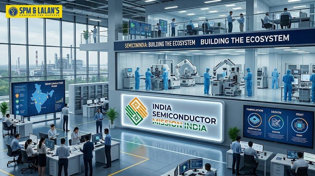
India Semiconductor Mission: Government Push for Chip Manufacturing
The India Semiconductor Mission is a major government push to strengthen the semiconductor industry in India, positioning India as a global hub for electronics manufacturing and design. It also serves as the nodal agency for the efficient and seamless implementation of semiconductor and display schemes.
The Objectives of the India Semiconductor Mission are-
- Strategy: Formulation of a comprehensive long-term strategy for developing semiconductors & display manufacturing facilities and a semiconductor design ecosystem in the country in consultation with Government ministries/departments/agencies, industry, and academia.
- Supply Chain: Facilitation in the adoption of trusted electronics through secure semiconductors and display supply chain, including raw materials, speciality chemicals, gases, and manufacturing equipment.
- Design & Start-Up: Enabling a multi-fold growth of the Indian semiconductor design industry by providing requisite support in the form of Electronic Design Automation (EDA) tools, foundry services, and other suitable mechanisms for early-stage start-ups.
- Intellectual Property: Promoting indigenous Intellectual Property (IP) generation and encouraging, enabling and incentivising Transfer of Technologies (ToT).
- Partnership: Enabling collaborations and partnership programs with national and international agencies, industries and institutions for catalysing collaborative research, commercialisation and skill development.
Major Semiconductor Sites in India
| Project | Location | Facility Type |
| Micron TechnologyLocation: Sanand | Gujarat | ATMP facility for DRAM and NAND products |
| Tata Electronics / TEPL with PSMCLocation: Dholera | Gujarat | Semiconductor fab |
| Tata Semiconductor Assembly and Test Pvt Ltd / TSATLocation: Morigaon | Assam | Semiconductor ATMP unit |
| CG Power with Renesas and Stars MicroelectronicsLocation: Sanand | Gujarat | ATMP unit for specialised chips |
| Kaynes Semicon Pvt LtdLocation: Sanand | Gujarat | Semiconductor packaging facility |
| HCL-Foxconn JV / India Chip Pvt LtdLocation: Near Jewar Airport, YEIDA | Uttar Pradesh | Display driver chip plant |
| SiCSem Private LimitedLocation: Info Valley, Bhubaneswar | Odisha | Silicon Carbide compound semiconductor fab |
| 3D Glass Solutions Inc.Location: Info Valley, Bhubaneswar | Odisha | Advanced packaging and embedded glass substrate unit |
| Continental Device India Ltd / CDILLocation: Mohali | Punjab | Discrete semiconductor expansion unit |
| Advanced System in Package Technologies / ASIPLocation: Andhra Pradesh | Andhra Pradesh | Semiconductor manufacturing unit |
| Crystal Matrix Limited / CMLLocation: Dholera | Gujarat | Compound semiconductor fab and ATMP facility |
| Suchi Semicon Private Limited / SSPLLocation: Surat | Gujarat | OSAT facility for discrete semiconductors |
What are the key areas in Semiconductor Engineering?
The Key areas of Semiconductor Engineering are-
- Chip Design: Chip design is the process of creating the structure of semiconductor chips. These chips are later used in phones, computers, vehicles, and electronic devices.
- Semiconductor Fabrication: Semiconductor fabrication means making chips inside special factories called fabs. This process needs advanced machines, clean rooms, and skilled engineers.
- Display Manufacturing: Display manufacturing focuses on making display panels for phones, laptops, televisions, vehicles, and digital screens.
- Compound Semiconductors: Compound semiconductors are used in high-performance electronic systems. They are useful in electric vehicles, telecom, power electronics and advanced devices.
- Silicon Photonics: Silicon photonics uses light signals to move data faster. Therefore, it is useful in high-speed communication, data centres, and advanced computing systems.
- Sensors and MEMS: Sensors and MEMS are tiny systems used in phones, vehicles, medical devices and smart machines. They help devices detect movement, pressure, temperature and other changes.
- ATMP and OSAT: ATMP and OSAT focus on chip assembly, testing and packaging. After a chip is made, this step prepares it for use in final electronic products.
What are the top jobs in the semiconductor industry?
The semiconductor industry in India offers many career options for engineering students. These jobs are not limited to only one area. Some of the top jobs in the semiconductor industry are given below-
- Chip Design Engineer: A chip design engineer creates the basic design of semiconductor chips
- Semiconductor Process Engineer: A process engineer works inside semiconductor fabs. Moreover, their main role is to improve the chip-making process and make sure the production runs smoothly.
- Semiconductor Manufacturing Engineer: Moreover, manufacturing engineers help in the actual production of chips. They work with machines, clean rooms, and production teams to maintain quality.
- Packaging Engineer: After testing, chips need proper packaging. Therefore, packaging engineers help protect the chip and prepare it for use in electronic products
- Test Engineer: A test engineer checks whether a chip is working properly or not. This role is very important because every chip must be tested before it is used in a device.
- Quality and Reliability Engineer: Quality engineers check the performance and safety of chips. They make sure that semiconductor products are reliable and can work for a long time.
What are the Courses to start a Career in Semiconductor Engineering?
To build a career in the semiconductor industry in India, students should start with courses related to electronics, chip design, VLSI and IC manufacturing that teach the basics of electronics, chip design, VLSI, and IC manufacturing. These subjects help them understand how tiny chips are created, tested, and used inside devices like phones, laptops, cars and smart machines.
Some of the Courses to start a Career in semiconductor engineering are given below-
- B.Tech Electronics Engineering in VLSI Design and Technology: Students planning to pursue Electronics and Communication Engineering through top institutes can benefit from structured JEE coaching in Guwahati to improve their chances of securing admission to leading engineering colleges.
- Diploma in IC Manufacturing: Students interested in the manufacturing area can choose a Diploma in IC Manufacturing. This course focuses on chip fabrication, clean room technology, semiconductor equipment maintenance, packaging, and testing.
- B.Tech in Electronics and Communication Engineering: This is the most common path to get into Semiconductor Engineering. This course builds a strong base in circuits, electronic devices, communication systems, and embedded systems.
- M.Tech in VLSI Design or Microelectronics: Students wanting deeper knowledge can go for M.Tech in VLSI Design, Microelectronics, or related fields. These courses are useful for careers in chip design, semiconductor research, testing, and advanced electronics.
- Online Courses through SWAYAM and NPTEL: SWAYAM and NPTEL are government-designed. These platforms offer courses from ITTs and IISC in engineering and technology areas.
What are the challenges of the semiconductor industry in India?
There are some major challenges to India’s Semiconductor Industry. Some of these are listed below-
- High Capital and R&D Cost: In setting a single advanced Semiconductor Fab costs upto 5 billion to 20 billion. This creates a major hurdle for domestic firms to come in
- Lack of skilled Workforce: While India has no shortage of chip design engineers (roughly 20% of the global pool), the country severely lacks hands-on, highly specialised manufacturing and shop-floor personnel
- Tech Gaps and global competition: Most Indian fabrication projects target mature technology nodes (e.g., 28nm), while the global demand and market focus have shifted toward highly advanced nodes (e.g., 3nm and 5nm)
Conclusion
The semiconductor industry in India is opening up a new path for growth, jobs and technology. From chip design to manufacturing, India is slowly building a stronger semiconductor ecosystem. At the same time, students can find new career options in VLSI, testing, packaging and fabrication. Therefore, semiconductor engineering is not just a technical field. It is also a future-ready opportunity for students who want to be part of India’s next big technology journey. Looking for more guidance on engineering careers, entrance exams, technology trends, and higher education opportunities? Visit SPM & Lalans for expert resources, career insights, and student support.
Sources: PIB, MeitY, India Semiconductor Mission(ISM)

SPM & LALAN’S Coaching is one of Assam’s leading institutes for JEE, NEET, Assam CEE, and Board Exam preparation. Established with a commitment to academic excellence, the institute provides expert faculty, personalized mentorship, comprehensive study materials, and a results-driven learning environment. Over the years, SPM & LALAN’S has helped thousands of students achieve success in competitive examinations and secure admissions to prestigious institutions across India. With a strong focus on concept-based learning, regular assessments, and student development, SPM & LALAN’S continues to be a trusted choice for aspiring engineers, doctors, and academic achievers throughout Assam and the Northeast.